Project Results
Overview
Our project was successful in creating a learning tool for those new to chess. The board would light up the correct available moves when a piece was picked up. It also successfully displayed checks and checkmate when they occurred. Our design was successful in handling pieces capturing other pieces as the game progressed.
Hardware Results
Hall Effect Results
The hall effect sensors were successful in capturing the positions of the squares with pieces on them. The first part of the entire board was getting the hall effect sensors to accurately sense where a piece was placed. All the hall effect sensor’s Vcc’s were wired in parallel across the row and DATA across the column to save on pins as we did not have 64 pins to read each. In Figure 1 we can see the output of the FPGA scanning through the hall effect’s rows.
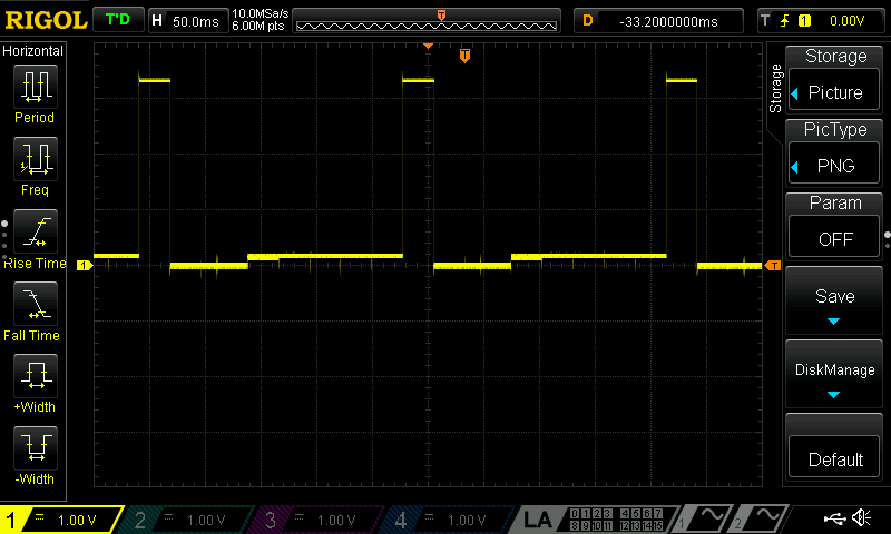
We are only checking one of the rows but can see that the FPGA is properly setting one row high 1/8 of the time and cycling through the others. We can then check the output of the columns to make sure that the hall effect matrix is outputting the correct data.
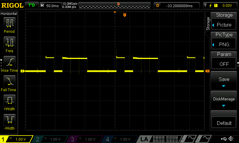
In Figure 2 we can see the column data of a column of tiles where one pawn has made one move. When a piece is on the hall effect sensor it will output a low signal and when there is no magnetic field it will output a high signal. So this properly captures where pieces are in the formation [XOXOOOXX] where X are pieces and O are empty squares. However the one thing is that the signal caps at a voltage of 1V. In order to fix this operational amplifiers were used giving us the trace in Figure 3.
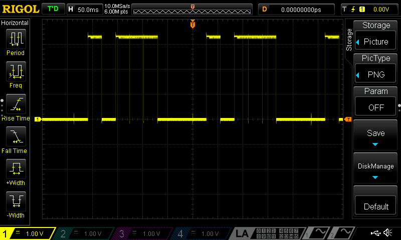
This looks much better and can be accurately read by the FPGA, proving our hall effect hardware worked as intended.
SPI Results
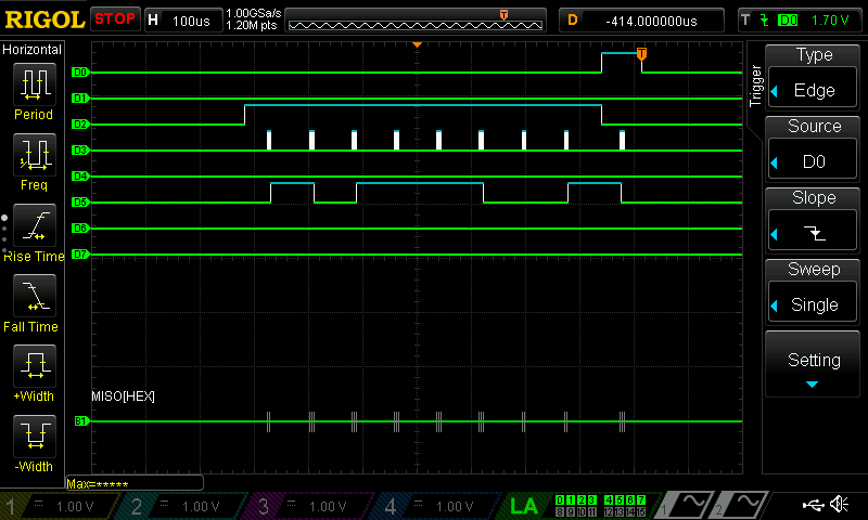
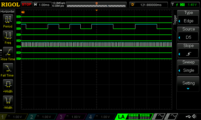
Once we are able to accurately read in data from the hall effect sensors on the state of the board we had to send this data over to the MCU using SPI. Figure 4 uses the logic analyzer and captures the SPI of board state as it is when the game starts.
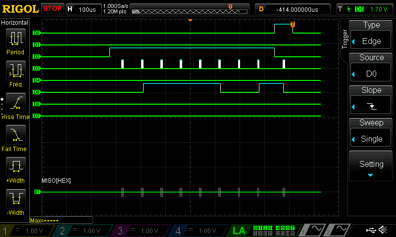
In Figure 4 D0 -> PA10 -> Load, D2 -> PA6 -> Done, D3 -> PB3 -> SCLK, and D5 -> PB4 -> MISO. We can see in the trace that as soon as Done goes high spi beings and we can see SCLK oscillate for eight transactions of 8 bits totaling the 64 bit board state. MISO is low for the first two transactions then high for four and low for the last two which is exactly how a chess board would look with 16 pieces in the first 16 tiles no pieces in the middle 32 tiles and 16 pieces in the last 16 tiles. After 8 transactions Load goes high to reset the FPGA’s SPI protocol setting Done low and one SPI transaction is completed before Load goes low and the cycle continues as it should.
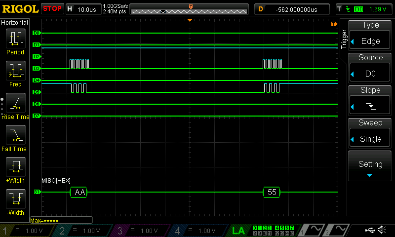
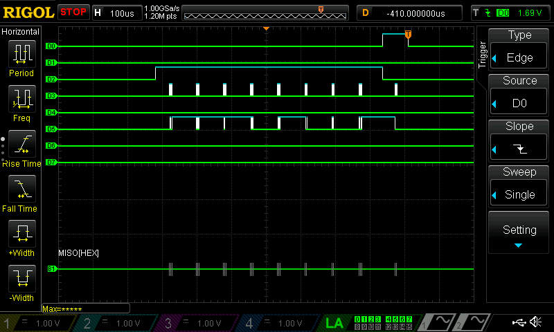
You can see some examples in the next few images.
LED Results
Once we know that the hall effect sensors were working and SPI was correctly sending the data over to the MCU the last step was to make sure the lights were being bitbanged correctly. Again we used the oscilloscope logic analyzer to capture when the LED was being sent data and clk.
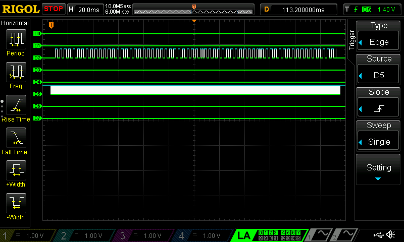
In Figure 5 D2 -> PB0 -> SDO and D5 -> PA9 -> CLK. We can clearly see the bit banged clock and data working as intended. If we zoom in more like in Figure 6 we can see that data changes correctly on the falling edge of the clock and that the clock has a duty cycle of 50%.
Chess Software Results
100% of the time, the board successfully lit up with the available moves for a piece. The board also displayed checks with 100% accuracy. Since the code for checking check was based on the last picked up and placed down piece’s direction, if one side was placed in check and one of its pieces was picked up and placed down, the light to signify check would no longer be lit. The board signified check mate accurately 100% of the time, as long as the pieces were moved one at a time, placed directly over magnet sensors, and in a legal(legal within the rules of chess) fashion. The software was able to successfully ignore erroneous signals from the board. Sometimes, the magnetic field from a piece would set of the sensor of an empty square adjacent to that piece’s square, and this was ignored in software by leveraging the fact that a signal of a piece being put down could only occur after a piece was picked up. Because the erroneous signal would signal a put down without a piece being picked up, ensuring a piece was picked up before a put down successfully evaded this error in signal.
Design in Action
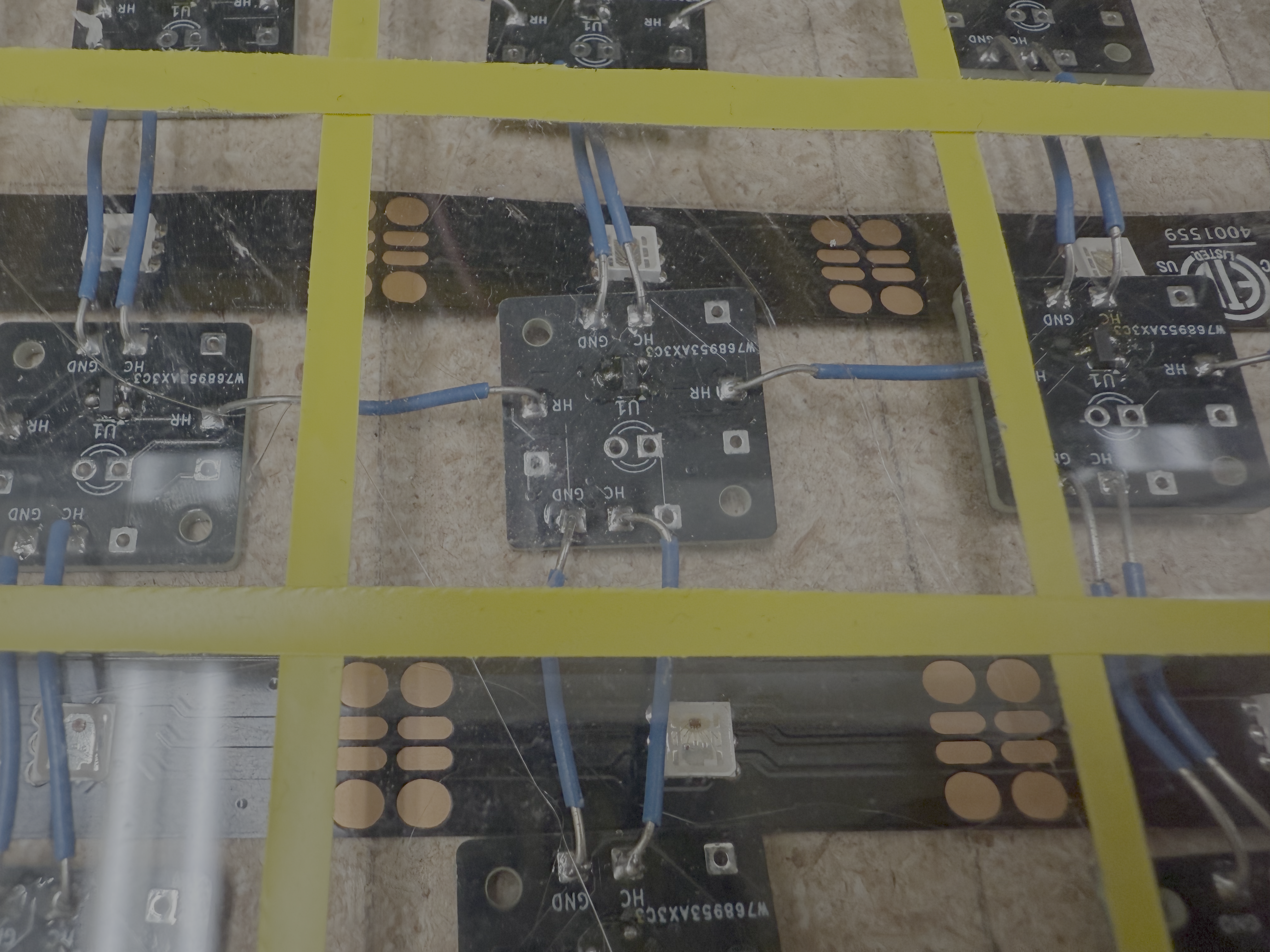
Figure 7 shows a picture of a chess board square with the designed PCB and LED on the LED strip under it.
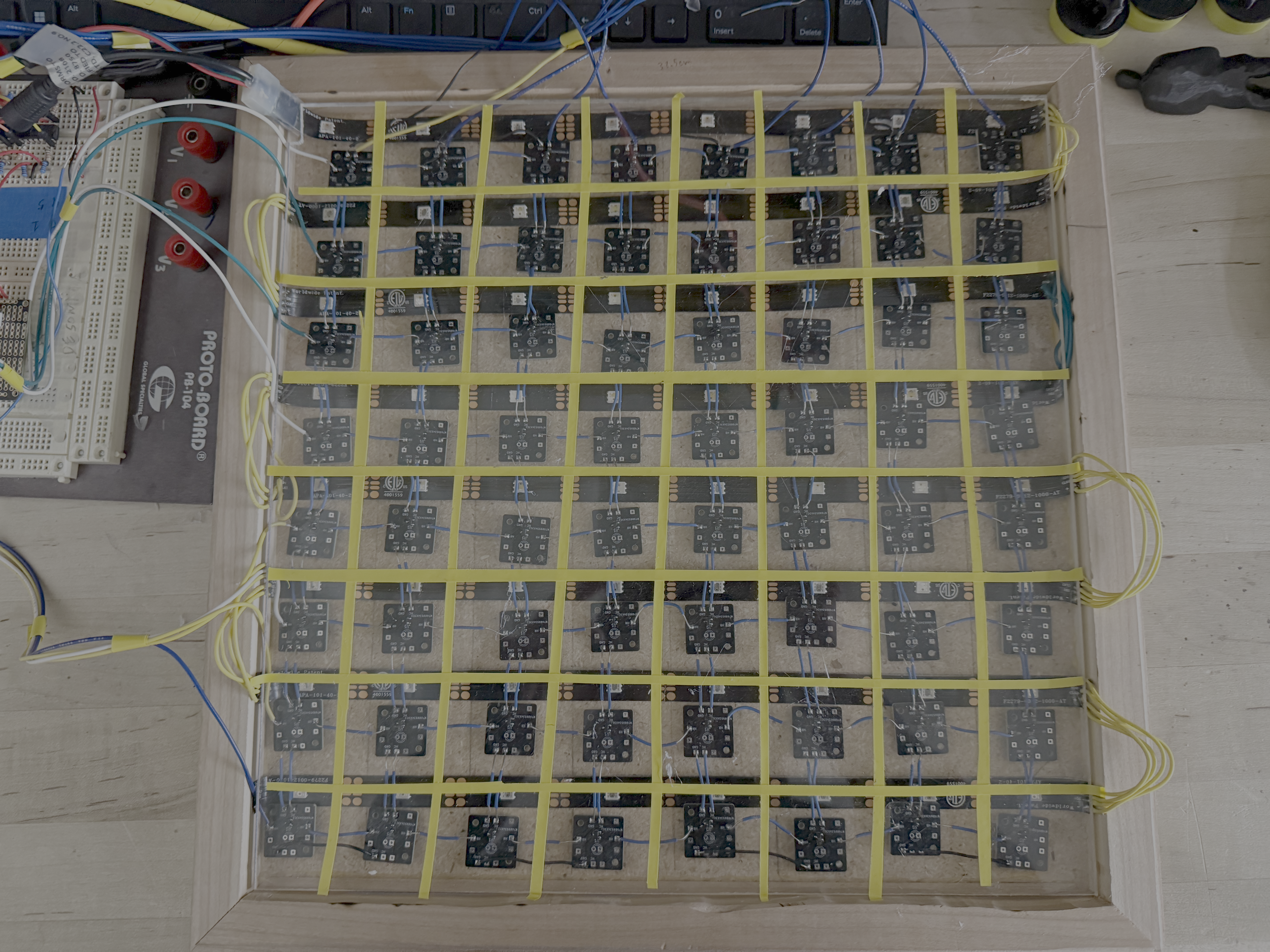
Figure 8 shows the circuit for the chess board.
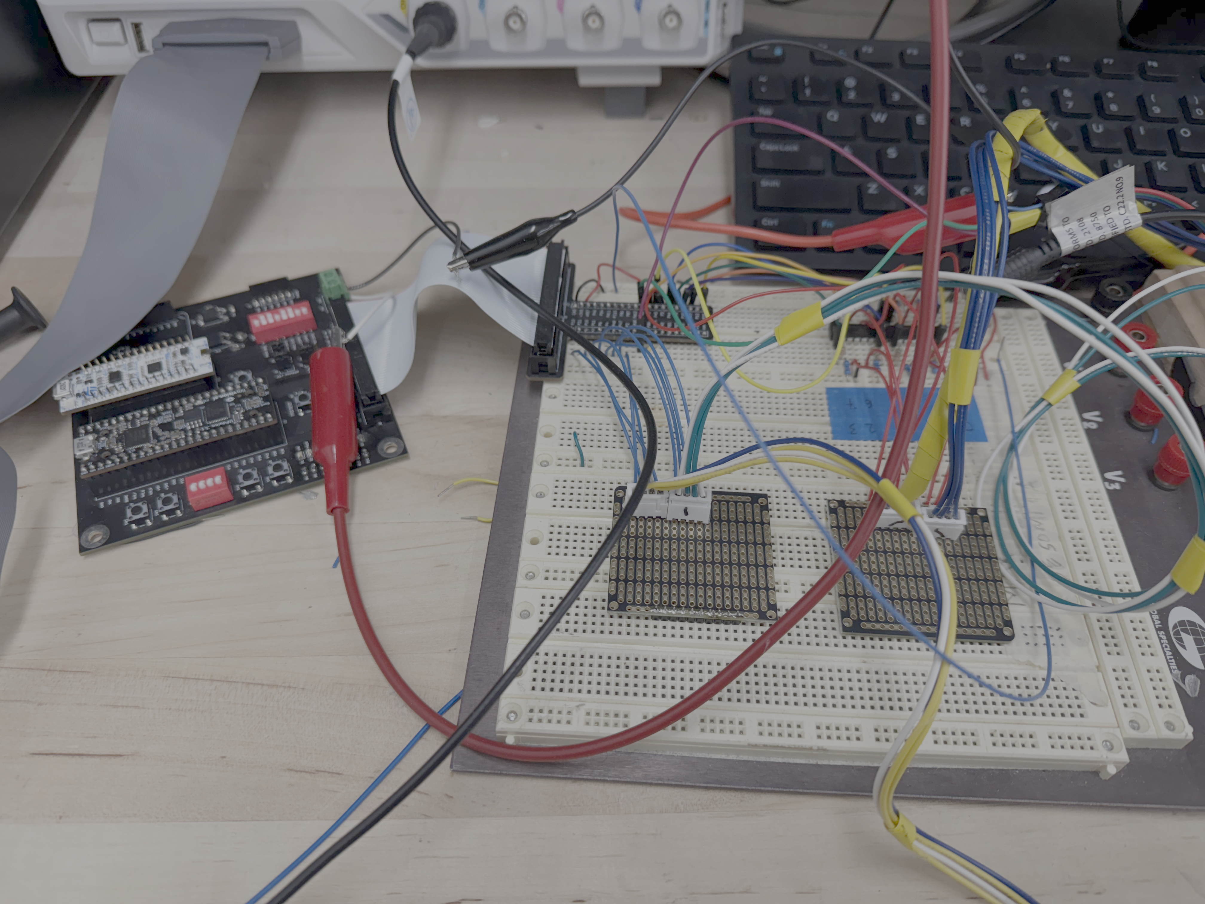
Figure 9 shows a picture of the circuit that includes the MCU and FPGA.
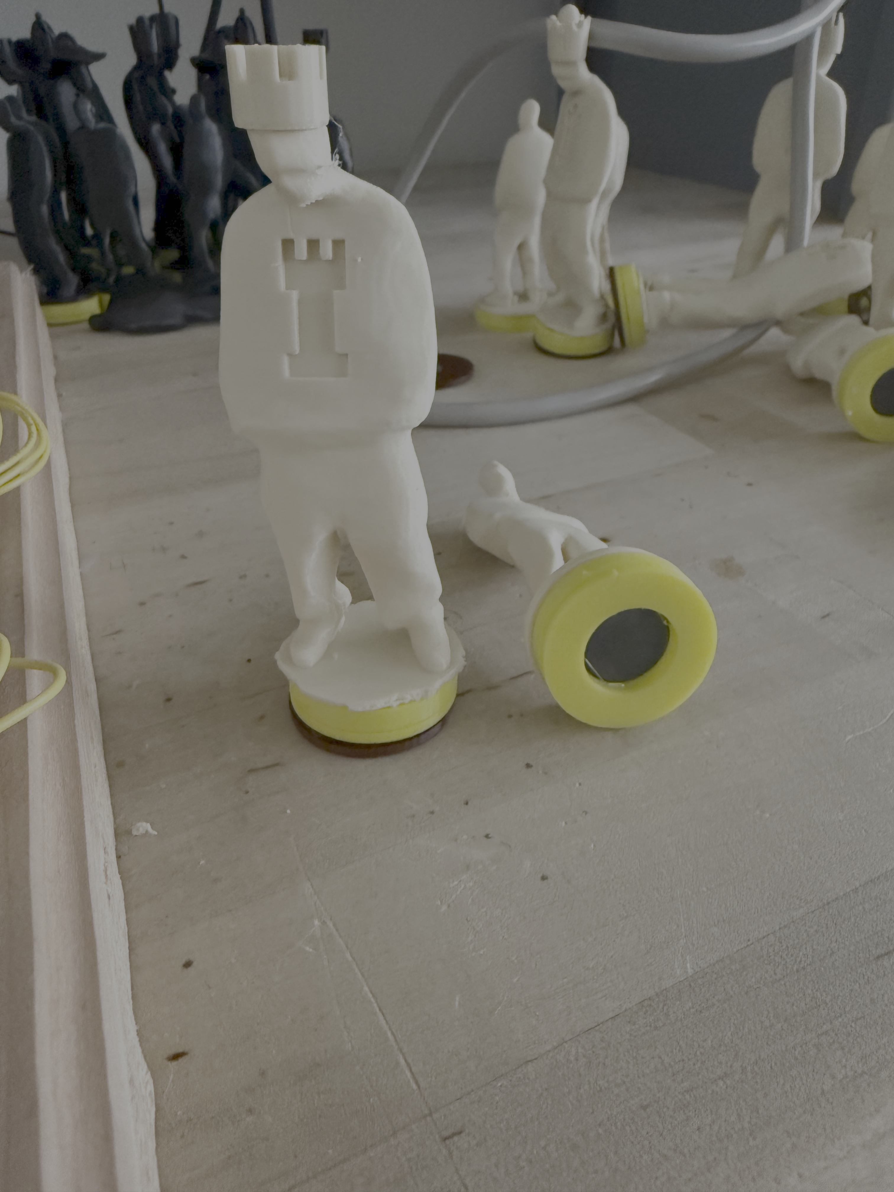
Figure 10 shows a picture of a rook piece, along with the magnet under each piece.
The above video shows the design handling each pieces movement correctly and a capture.
The above video shows the design handling a check correctly.
The above video shows the design handling a checkmate correctly.