FPGA Design
FPGA Role
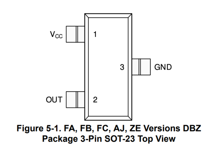
The role of the FPGA in this project was to interact with the hall effect sensors. The SMT hall effect sensors we used were a new hardware that needed to be powered with 3.3 V on Vcc and ground on GND. Once powered they had an OUT pin that would provide a high signal in the absence of a magnetic field and a low signal if a magnet was nearby.

The hall effect sensors were arranged in a matrix. This allowed us to wire all the Vcc pins in parallel across the rows and the OUT pin in parallel across the columns. This design significantly saves on wires. Instead of needing 64 wires for each data pin and 64 for each power, only 8 wires were needed for data and 8 for power. Each of the eight row pins was powered one at a time and the packet of eight column pins was recorded. The packets could then be stitched together to create the current state of the board indicating where pieces are.
Once the FPGA successfully scans through the rows and calculates the board state, it simulates the SPI protocol to send the board state over to the MCU. The MCU is then in charge of taking that board data and turning on specific LED’s and updating the current state. The FPGA continually sends SPI packets to the MCU as the MCU loops through its while loop to make sure it has up to date board data.
FPGA System
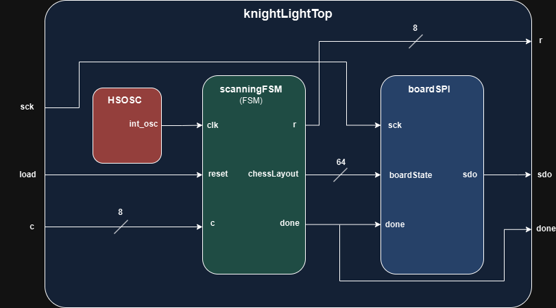
The FPGA follows the block diagram shown below.

There are two main modules scanningFSM and boardSPI.
scanningFSM
scanningFSM has three inputs clk, reset, and c. clk drives the fsm which is a slowed down version of int_osc from the HSOSC module. reset is received from the top level module input load which is set by the MCU when it begins a new SPI request. Lastly c is the packet of 8 bit column data from the hall effect matrix.
It also has three outputs r, chessLayout, and done. r is connected to the rows of the hall effect matrix turning the Vcc of each row’s hall effect sensors on one at a time. chessLayout is a 64 bit value that represent which tiles have pieces on them and is created by stitching together c at different timing. Lastly done is a signal that is sent to the mcu that tells it when the FPGA has stable board data and can send it over spi.
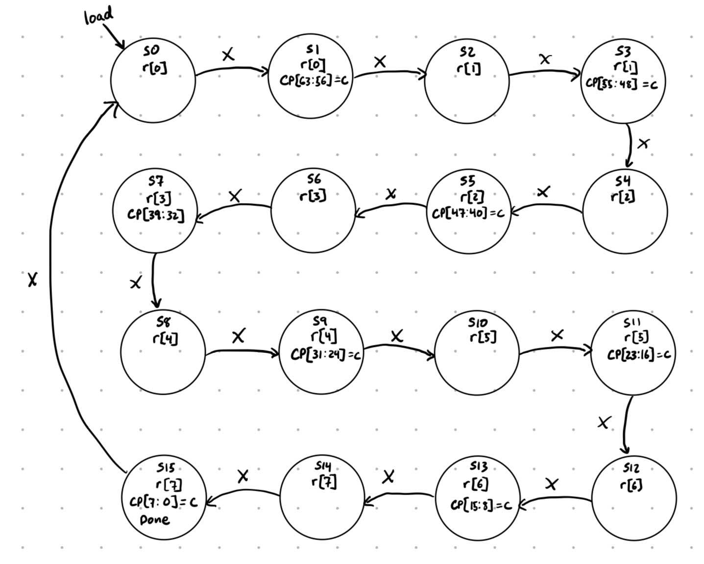
The FSM follows the diagram below.  The FSM has 16 states and at every clock cycle it goes to the next state regardless of any input. Every two states it drives a different row high powering them one at a time allowing the FSM to scan through the hall effect matrix. On the second of every two states it also records the the current column data to
 chessPieces which I abbreviate CP. Since all the DATA pins are wired in parallel when the column is recorded it should only receive data from the specific row that is being powered by the FSM. We decided to record the data at the second state that the specific row was high as the data from the hall effect was less stable when first powered on, thus the second state allowed it to become stable before recording. Lastly once the FSM has traversed through all 16 states the done flag is set high and the output chessLayout is set to chessPieces.
boardSPI
boardSPI has three inputs sck, boardState, and done. sck is ported from the mcu as the SPI clock. boardState comes from scanningFSM once it has collected the board date. Lastly done is received from scanningFSM and indicates to this module that boardState is stable and ready to sent over to the mcu. There is only on output which is ‘sdo’. This module uses a custom SPI protocol similar to lab 7 that shifts out sdo one bit at a time on the negative edge of sck sending it over bit by bit.