Lab 2: FPGA and MCU Setup and Testing
Introduction
In this lab we learned how to use time multiplxing to efficiently use the I/O on our FPGA.
Lab Overview
The goal for this lab was to power two seven segment displays using seven output pins, by using time multiplexing. In addition to using time multiplexing to run two seven segment displays, transistors were used to drive large currents to the common annodes of the seven segment displays. This allowed pins on the FPGA which aren’t capable of driving large currents themselves to use the transistors as a switch allowing the FPGA to toggle the displays on and off quickly.
Design Approach
Time multiplexing is a way to share expensive hardware for different purposes using specific timing. We used multiplexing in this lab by driving two seperate seven segment displays using only seven pins. How it works in this lab is that the same signal (i.e., the same hexadecimal number) is sent to both seven segments. However, two FPGA pins are used to control the common annode’s on either display, toggling one off while the other is on, and synchonously switching the hexadecimal output with the pwoer toggle at around 240 Hz to make it look as if there are two distinct numbers. Both displays are controlled by their own quad dip switch input, and lastly the sum of both numbers are displayed as a five bit number on five seperate LEDS.

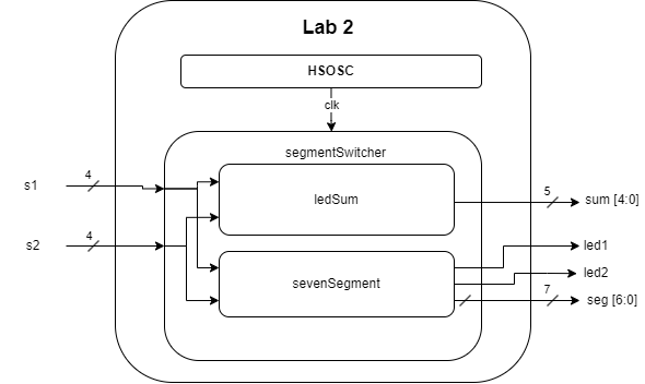
The systemVerilog code that was flashed onto the fpga followed the block diagram below. The top module Lab 2 has inputs s1 [3:0] and s2 [3:0] which come from each of the quad dip switches. Those inputs then enter ledSum which is just an adder summing the two inputs into sum [4:0]. s1 and s2 also enter the sevenSegment module in addition to the clk signal which comes from the HSOSC. The sevenSegment module then alternates between turning on the left or right led segment using led1 and led2 outputs which are connected to the transistors as well as outputts the correct seg [6:0] output to light up specific segments on the display. led1 and led2 are toggled based on the 4.8 MHz clk signal which is modified to effectively act as a 240 Hz clock which flips led1 and led2 every cycle.

Testing Approach
To test the modules discussed above a testbench was used to run a device under test. This test bench was quite simple compared to the last lab and did not use test vectors but instead was used to monitor when led1 and led2 toggled on or off and if the correct seg[6:0] was outputted depedning on which segment was powered. The DUT ended up being the segmentSwitcher module. Initially I planned to test each module seperately however the sevenSegment module was tested last week and ledSum just summed two inputs, so I decided to test all of segmentSwitcher. The systemVerilog used is provided below.
module segmentSwitcher_tb();
 // Set up test signals
 logic clk;
 logic [3:0] s1,s2;
 logic led1, led2;
 logic [4:0] sum;
 logic [6:0] seg;

 // Instantiate the device under test
 segmentSwitcher dut(.s1(s1),.s2(s2), .clk(clk), .led1(led1),.led2(led2), .seg(seg), .sum(sum));

 // Generate clock signal with a period of 10 timesteps.
 always
   begin
     clk = 1; #5;
     clk = 0; #5;
   end

initial
 begin
    // test different inputs
    s1 = 4'b0000;
    s2 = 4'b1111;
    #20;
    s1 = 4'b1000;
    s2 = 4'b0001;
    #20;
    s1 = 4'b1010;
    s2 = 4'b1001;
    #20;
 end
endmodule
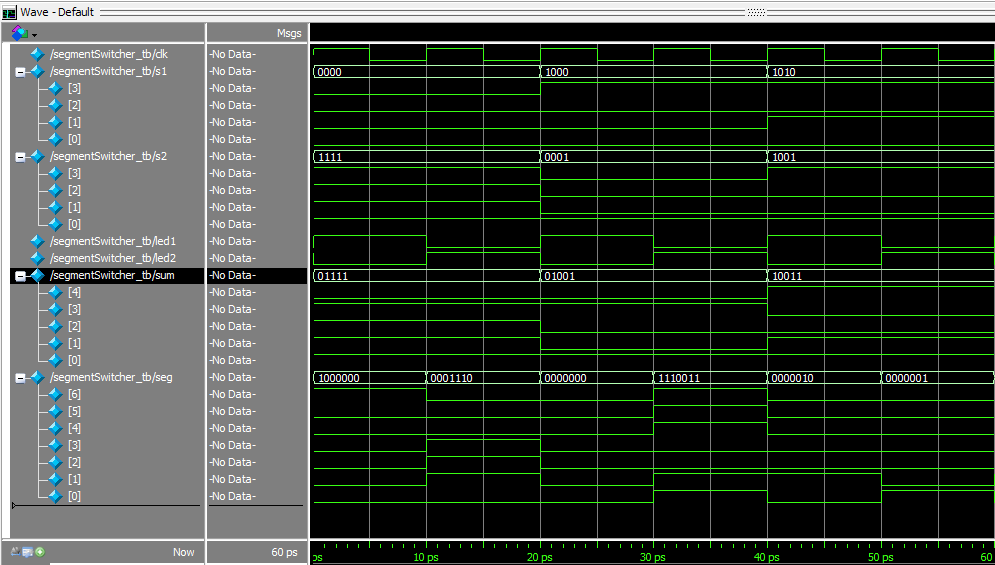
The results from the wave function can be seen below. We can see that led1 and led2 oscillate oppositely as intended. In addition seg correctly outputs s1 if led1 is high and s2 if led2 is high. Lastly the summing module successfully sums s1 and s2 together and outputs it to sum.

Wiring up the Board
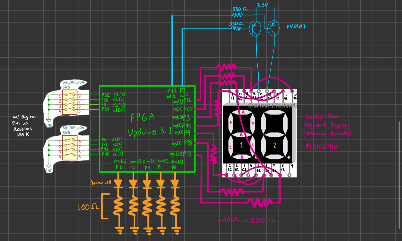
After writing the system verilog modules and thoroughly testing them in a testbench it was time to wire of the FPGA. The FPGA was wired according to the pin layout below. The transistors used were PNP transistors (PN 2907). These were used to drive the common annodes of the displays to 3.3V and were switched on when P47 and P2 were driven low.  Again resistors were used to limit the current for the I/O pins and the LEDs. The work for calculating the transistor base resistor, the seven segment resistor, and the yellow led resistor are shown below. The data sheet states that the recommended current for the FPGA I/O should be 8 mA. The transistor uses a diode that has a forward foltage of 0.7 V, from there we can calculate the resistance we need to set the current to 8 mA. The resistance ended up being 325 Ohms, which was close enough to the 330 Ohm resistors found in the lab. The seven segment display has a forward voltage of 1.8 V and the target amperage was 8 mA again, resuling in a resistance of 163 Ohms which was close to the 200 Ohm resistor in the cabinet. lastly for the yellow LEDs, I wanted them to be bright so I targeted a higher current of 15 mA, which correlates to a 100 Ohm resistance. Lastly for the addition quad dip switch used in this lab, internal FPGA pull up resistors of 100 kOhm were used.
Outcome
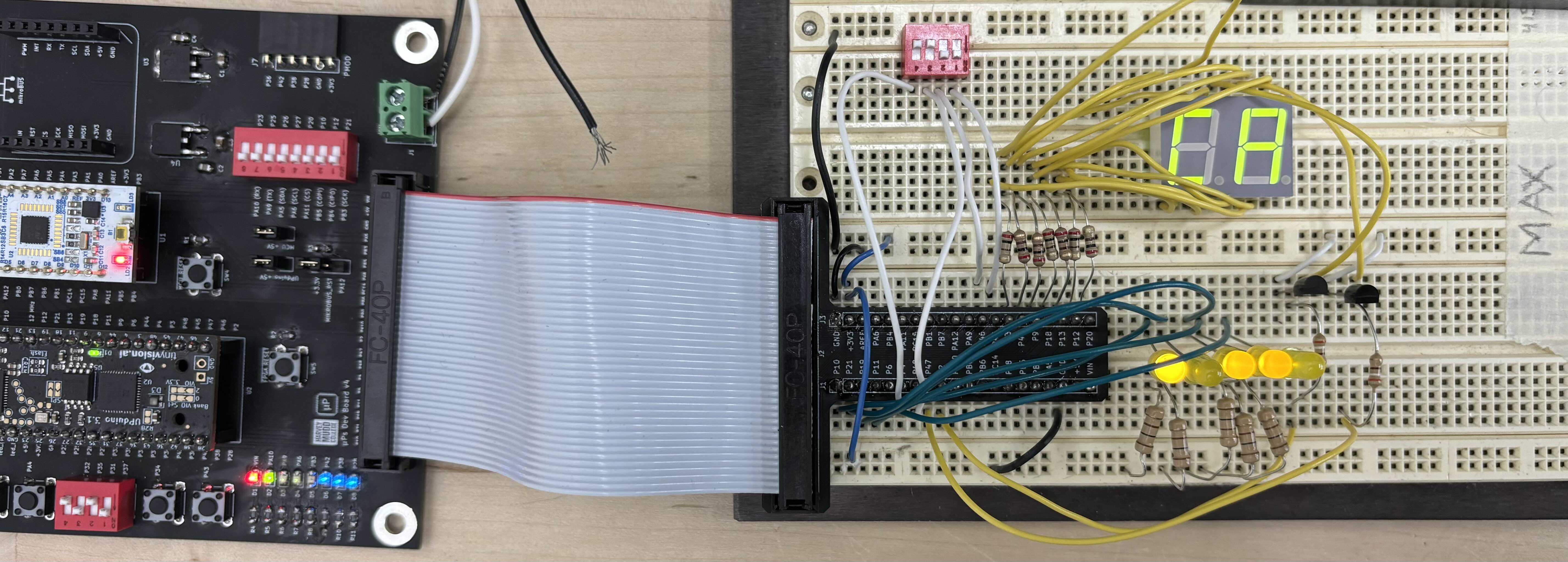
Below you can see a video of the working double seven segment display as well as the five LEDs showing the sum of the two hexadecimal number. This lab turned out successfully as all requirements were met including multiplexing two seven segment displays off of a single seven segment module using transistors, displaying the correct output depending on the input, and finally not having any visual flickering or bleeding.
Hours in lab this week: 16 hours