Lab 1: FPGA and MCU Setup and Testing
Introduction
In this lab we soldered our E155 protoboard, tested our FPGA and MCU, and created our own FPGA design to drive onboard LEDs as well as a seven segment display.
Development Board
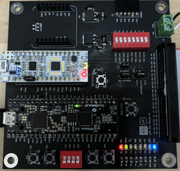
For the development board we were given we soldered a variety of surface mount technology (SMT) and through hole technology (THT) components. The brains behind the development board consisto of the UPduino v3.1 FPGA and Nucleo-L432KC MCU which were attached through header pins. Additionally switches, voltage regulators, and jumpers to set power for the MCU and FPGA were added to the board. The most difficult part was soldering all the SMT leds, capacitors, and resistors as it was tricky to get them in the correct place with how small they were.
Testing the FPGA and MCU
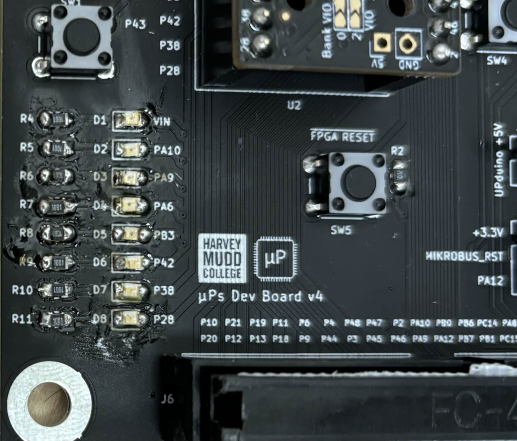
The FPGA and MCU were then tested to make sure they worked properly along with all the soldered components on the PCB. They were able to be test by using the onboard PCB LEDs which connect internally to specific pins of the FPGA and MCU. For my board I found that three of my LEDS and one of the current limiting resistors needed to be reflowed. However after reflowing, and using Radiant to program the FPGA and Segger to program the MCU it worked worked succesfully.
FPGA Design
Lab Description
After I had thoroughly tested that my FPGA, MCU, and development board, I designed FPGA modules to control different LEDs. The task was to light up the LED’s and a seven segment display depending on what dip switches were selected, described more in the table below.
| Signal Name | Signal Type | Description |
|---|---|---|
s[3:0] |
input | the four DIP switches (on the board, SW6) |
led[2:0] |
output | 3 LEDs (you may use the on-board LEDs) |
seg[6:0] |
output | the segments of a common-anode 7-segment display |
Two of the LEDs, led[0] and led[1], were designed accordingly:
s1 |
s0 |
led[0] |
|---|---|---|
| 0 | 0 | 0 |
| 0 | 1 | 1 |
| 1 | 0 | 1 |
| 1 | 1 | 0 |
s3 |
s2 |
led[1] |
|---|---|---|
| 0 | 0 | 0 |
| 0 | 1 | 0 |
| 1 | 0 | 0 |
| 1 | 1 | 1 |
led[2] did not follow a truth table but instead was designed to blink at 2.4 Hz.
As for the seven segment display it needs to read in the dip switch signals and display the four bit binary number as a single hexadecimal number on the seven segment display. For example if the dip switch input s[3:0] was 0110 the seven segment display must show a 6 while if it was 1101 it would display a d.
Design
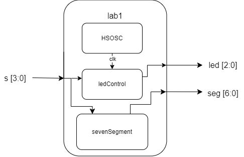
Below is the block diagram used to design the combinational logic that that drove both the LEDs and seven segment display:
LED Design
To design led[0] and led[1] we can clearly see that led[0] is simply an exclusive or (XOR gate) of input s0 and s1. While led[1] is an and gate of s2 and s3. For led[2] it was necessary to make sure it blinked at 2.4 Hz. This means that every cycle of led[2] will last around 0.4167 seconds. Using a duty cycle of 50%, the LED needs to switch on or off every 0.2083 seconds. The HSOSC library was utilized to create a clock that oscillated at 48 Mhz meaning it ticks every \(2.083*10^-8\) seconds. This meant that it would take \(10^8\) ticks to complete a half cycle for led[3]. To design this a flip flop was used that counts every tick and switched the led on or off every 10,000,000 counts.
Seven Segment Design
To design the seven segment display the SystemVerilog module used a submodule which had an input of s[3:0] and an output of seg[6:0]. This submodule comntained a case statement with 16 cases, one for each off the possible dip switch combinations (4’b000, 4’b0001, … , 4’b1111). Once the SystemVerilog checked the case it would then turn off the specific pins that correlated to the specific segments to create each hexadecimal number. One interesting point about the seven segment display is that it was common annode, meaning it had one common pin at 3.3V, meaning the FPGA must drive the desired pin to low to light up the particular segment.
Testing
A test bench was used to test the SystemVerilog code was working according to the proposed design. The testbench ran all 16 cominations of the dip switches and tested the expected led[3:0] and expected seg[6:0] outputs vs what the actual output of the modules would be in simulation.
// sevenSeg_testvectors.tv
// Max De Somma
// mdesomma@g.hmc.edu
// 9/3/24

// [3:0]s, [2:0]led, [6:0]segment
0000_000_1000000
0001_001_1110011
0010_001_0100100
0011_000_0100001
0100_000_0010011
0101_001_0001001
0110_001_0001000
0111_000_1100011
1000_000_0000000
1001_001_0000001
1010_001_0000010
1011_000_0011000
1100_010_1001100
1101_011_0110000
1110_011_0001100
1111_010_0001110
The test vector file above was the one used in the testbench that had the correct output for every case. Every test passed proving the SystemVerilog code worked correctly.
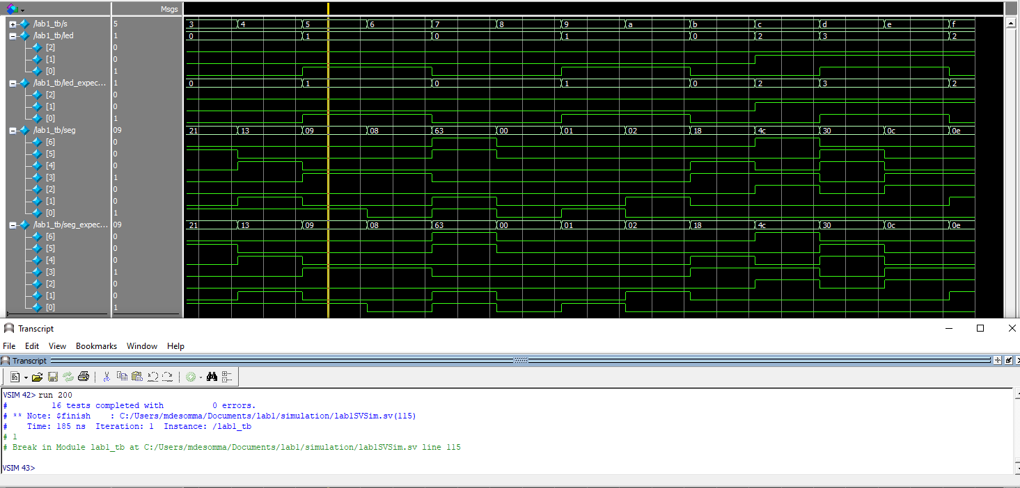
However the testbench fell short as led[2] was not able to be tested which is clear in the photo above. This was due to the fact that the HSOSC libary was not include in model sim. However it was possible to validate it using an oscilloscope proving it oscillated between 0 V and 3.3V at a freq of 2.42 Hz which is close to the desired 2.40 Hz. 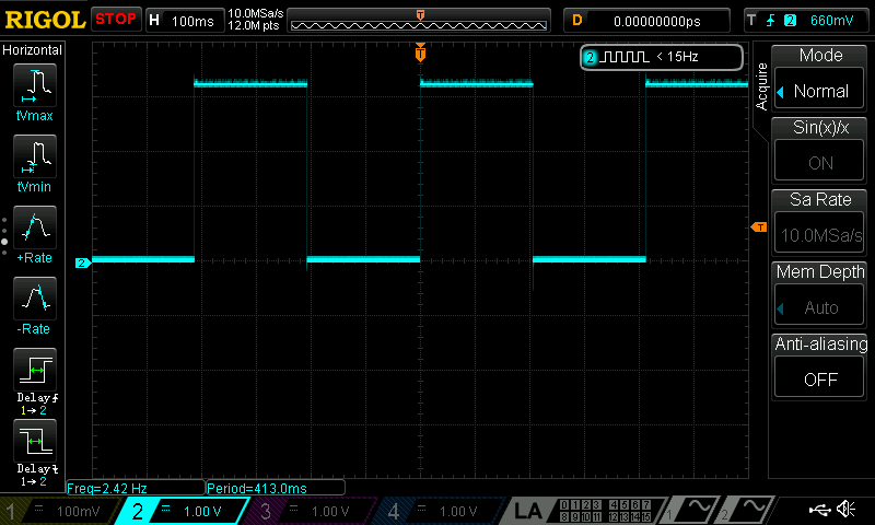
Wiring and Outcome
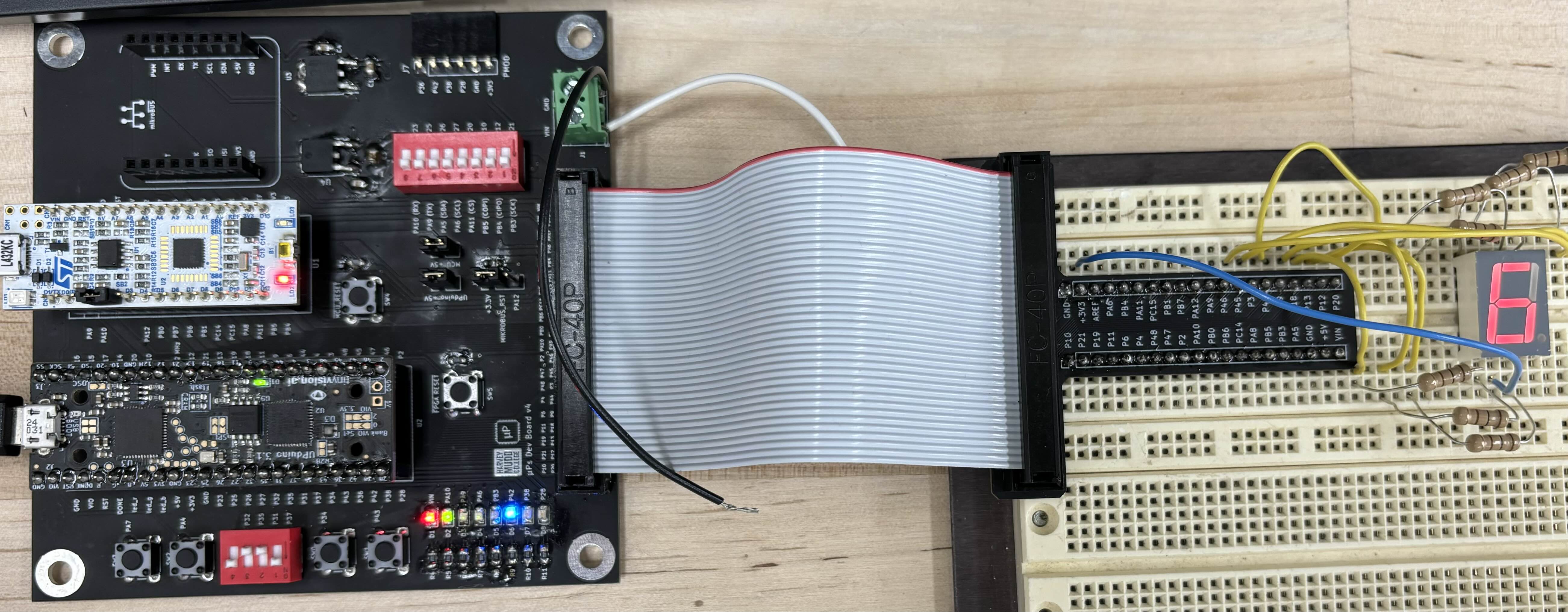
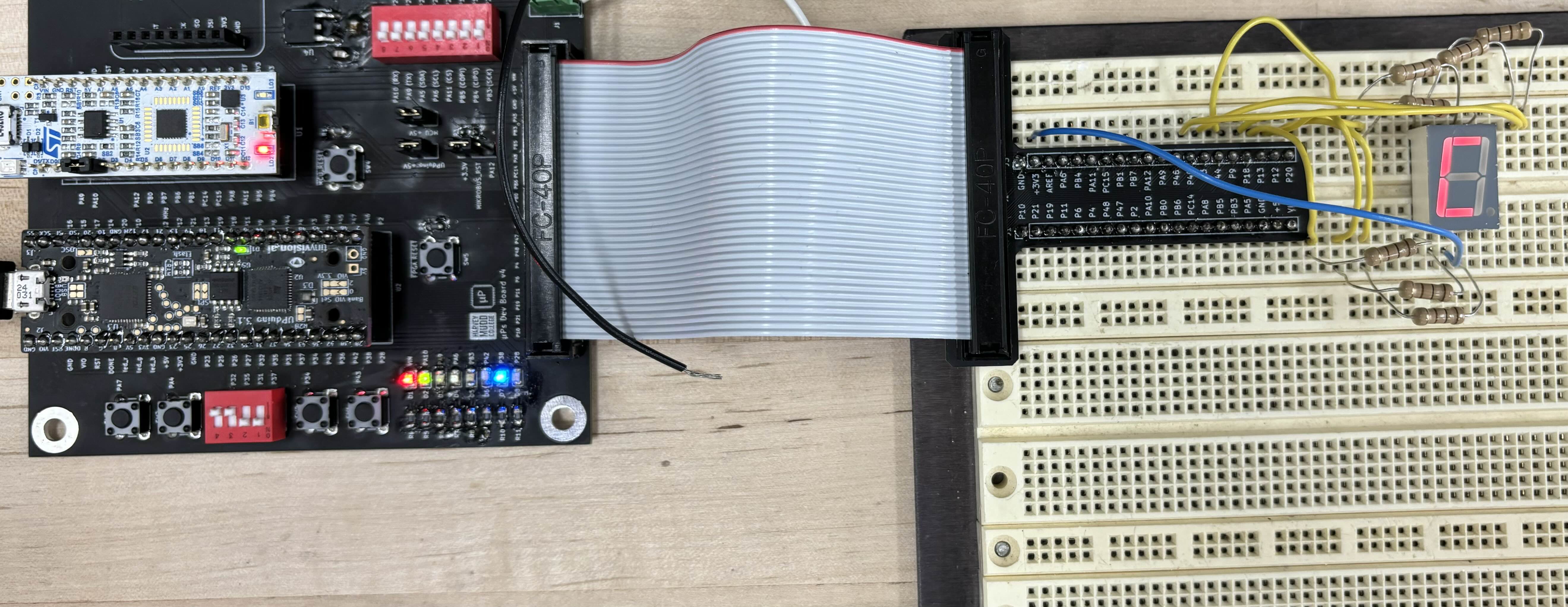
After writing and testing the SystemVerilog, it was time to connect the LED’s and Seven Segment to my FPGA using the following wiring schematic.
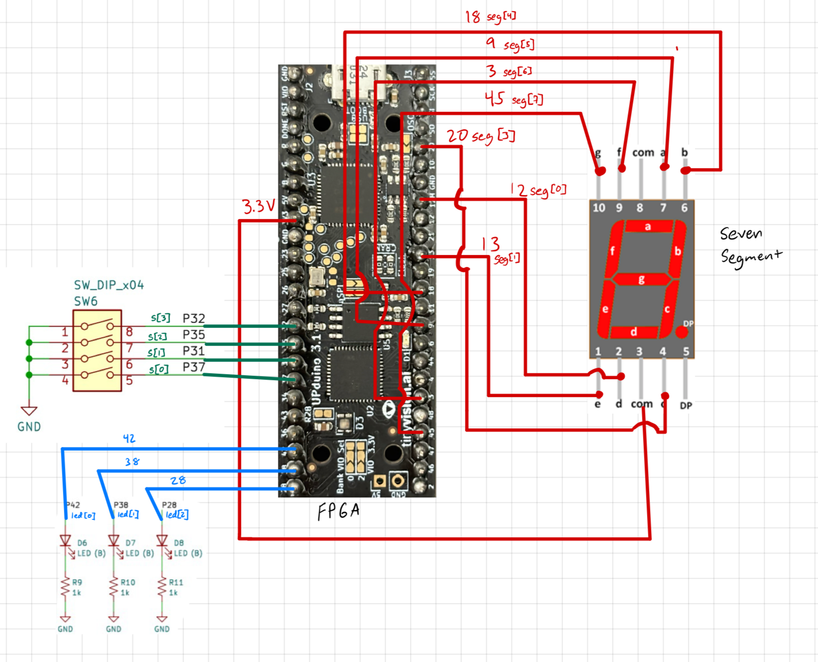
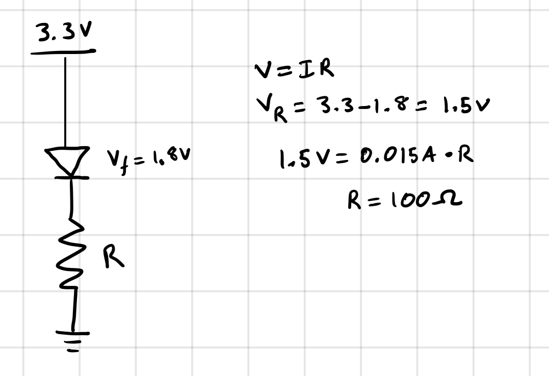
However to prevent the seven segment drawing too much current, current limiting resistors were added to all seven seg[7:0] pins targeting 15 mA. On the seven segment data sheet, it stated that the red led segments had a forward voltage of 1.8 V. This meant that voltage across the resistor would be 1.5 V, and thus could use V = IR with a target current of 0.15 mA to calculate R.
After finally wiring all the inputs and the output to the FPGA and downloading the SystemVerilog module to the board the development board was succesfully able to drive the seven segment display and display the correct hexadecimal number and proper onboard LEDs. Additionally as shown above the led[2] blinked at the correct 2.4 Hz. This wraped up Lab 1, verifying that the development board worked properly while giving me a chance to design my own FPGA modules. In total this lab took 21 hours.
